



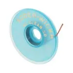
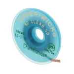
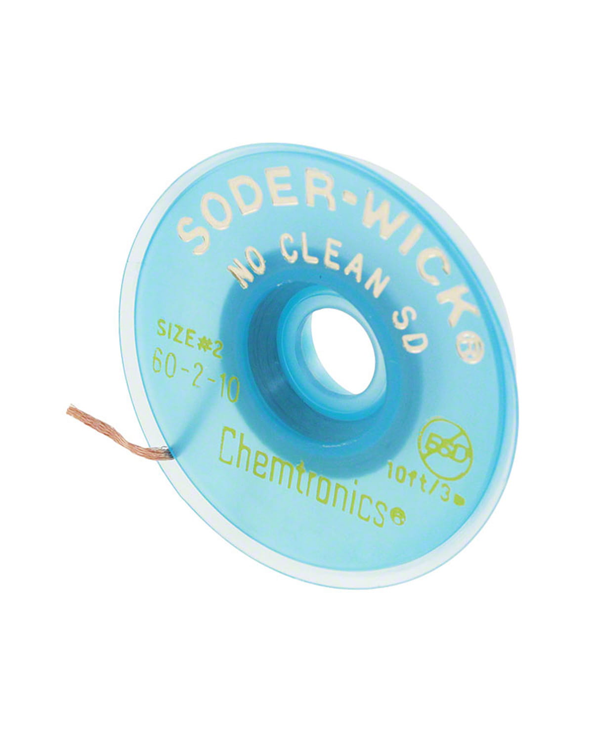
NO CLEAN SD desoldering wick 1.3 mm 3 m
11,50 € VAT ExcI.
NO CLEAN SD desoldering wick in pure oxygen-free copper, width 1.3 mm / 0.050″, length 3 m / 10 ft. Ideal for removing excess solder from PCBs, medium-sized SMD pads, and small PTH components.
| Weight | 0,01 kg |
|---|---|
| Dimensions | 4 × 4 × 1 cm |
| FLT-Soldering-Product Typ | Desoldering Braid |
| FLT-Lead Free | Yes |
| FLT-Soldering-Flux | No-Clean |
| FLT-Package | Coil |
| FLT-Size | 1.3mm (0.05'') |
| FLT-Quantity | 3m (10') |
In stock (can be backordered)
The 1.3 mm NO CLEAN SD desoldering wick is designed for the rapid and controlled removal of excess solder from printed circuit boards and electronic components.
The 1.3 mm / 0.050″ size, corresponding to Size #2, is particularly suitable for work on medium-sized SMD pads and small PTH through-hole components, where greater absorption capacity is required compared to finer wicks.
The braid is made of pure oxygen-free copper and uses a non-corrosive, halide-free, organic-based NO CLEAN SD flux technology. This formulation enables effective desoldering, reducing harmful residues and leaving the PCB clean and ready for component repositioning or new soldering.
The braid’s low-mass construction and high thermal conductivity provide a fast response even at lower temperatures, limiting the risk of overheating and damage to the printed circuit board.
Perfect for:
- Removing excess solder from PCBs
- Cleaning of medium-sized SMD pads
- Small PTH through-hole components
- Rework and electronic repairs
- Preparing the PCB before component repositioning
- Fast desoldering with reduced risk of overheating
- Electronics labs and technical service centers
- Use where more absorption capacity is required compared to Size #1
| Feature | Description |
|---|---|
| Product code | SLD-SLW-002 |
| Product type | Desoldering braid |
| Technology | NO CLEAN SD |
| Size | Size #2 |
| Wick width | 1.3 mm / 0.050″ |
| Length | 3.048 m / 10 ft |
| Material | Pure oxygen-free copper |
| Flux type | Organic no-clean, non-corrosive, and halide-free |
| ANSI/IPC J-STD-004 classification | ROL0 |
| Residues | Reduced, suitable for no-clean processes |
| Recommended applications | Solder removal from PCBs, medium-sized SMD pads, and small PTH components |
| Main advantage | Greater absorption capacity compared to Size #1, while maintaining good operational precision |
Only logged in customers who have purchased this product may leave a review.
Related products
Microchip 25LC256 SPI EEPROM Memory SO8
Available on backorder
Reviews
There are no reviews yet.